Rigorously tested signal magnetics, integrated RJ45 modular jacks, and high-speed SFP transceivers engineered for zero packet loss and low latency.
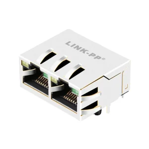
An engineering-level examination of Layer 1/Layer 2 connectivity, OEM selection matrices, and signal isolation physics.
In contemporary enterprise communications and cloud-scale data center architectures, the term "Network Hub" has evolved beyond legacy multiport physical repeaters. Today, enterprise procurement officers and lead network architects evaluate physical-layer infrastructure based on integrated magnetic connector topology, EMI/RFI suppression capabilities, and multi-gigabit optical transceivers capable of handling ultra-low-latency data throughput.
Selecting top trusted network hub factories and exporters requires evaluating direct component-level precision. Modern Ethernet devices demand flawless coupling transformers, specialized SFP+ cages, and high-density modular jacks. As global enterprises shift toward AI cluster computing, high-frequency automated trading, and industrial IoT (IIoT), the underlying component infrastructure must guarantee 100% bit error rate (BER) efficiency under harsh operating environments.
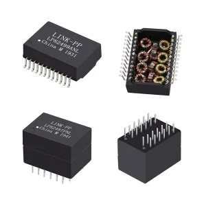
Key Engineering Insight: Signal integrity at the PHY layer is governed by magnetic isolation performance. Integrated Magnetics Jacks (ICM) reduce PCB space by 50% while mitigating electromagnetic interference through precisely tuned toroidal cores and common-mode chokes.
Historically, network hubs operated purely at Layer 1 of the OSI model, broadcasting signal packets indiscriminately across all active ports. Modern network hub manufacturing, however, encompasses the design and fabrication of complex physical interface modules—including multi-port ganged SFP cages, PoE-enabled magnetic jacks, and high-bandwidth optical transceiver assemblies.
Leading global manufacturers focus on three critical technical pillars:
Detailed insights into physical layer interconnect components required for mission-critical deployments.
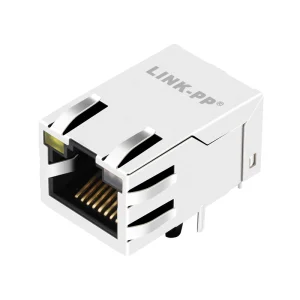
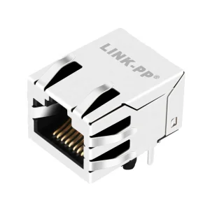
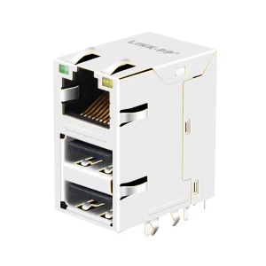
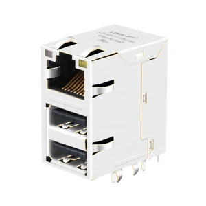
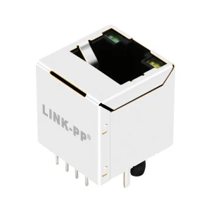
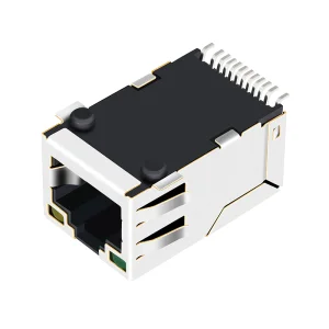
Combines RJ45 connectors with transformers, chokes, and capacitors. Eliminates discrete component layout on the main system PCB, improving return loss performance and reducing board footprint.
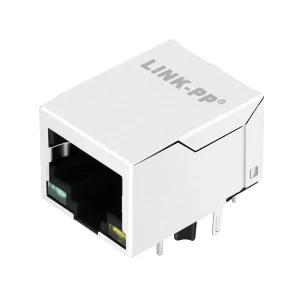
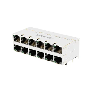
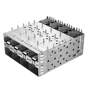
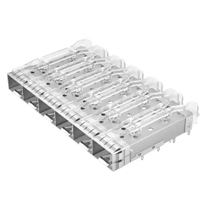
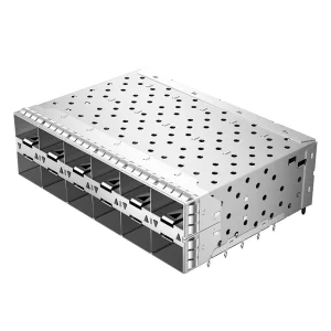
High-density ganged configurations (such as 2x4 and 2x6 ports) with enhanced EMI shielding fingers. Designed for press-fit PCB mounting to ensure mechanical robustness and minimal RF leakage.
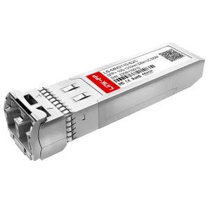
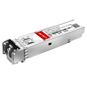
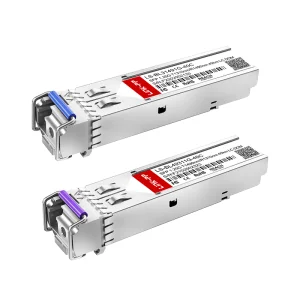
From 1G BiDi single-mode solutions up to 10GBASE-LRM multi-mode modules. Built on Multi-Source Agreements (MSA) to ensure drop-in interoperability with Cisco, TE, and Tyco switch architectures.
A verified high-tech manufacturer specializing in optical modules, magnetic connectors, and network hub interface hardware.
Established in 2016, FiberNova Optical Communication Tech Co., Ltd. (FiberNovaTransceivers.com) operates a specialized manufacturing facility covering approximately 380㎡ dedicated to high-precision optical transceivers and modular magnetic components. Combining 12 years of core industry expertise with over 6 years of dedicated international export experience, FiberNova generates an annual export volume ranging between USD 8 million and 15 million.
FiberNova's global tier-1 supply chain covers North America, Europe, Southeast Asia, and the Middle East, with core markets including the United States, Germany, Japan, South Korea, and the United Arab Emirates. Supported by an ecosystem of over 1,200 upstream supply chain partners, FiberNova maintains stable sourcing for high-grade silicon photonics chips, semiconductor lasers, planar lightwave circuits (PLC), and precision magnetic cores.
Quality assurance is backed by a team of 45 professional QC specialists enforcing 100% optical performance testing, rigorous thermal chamber cycling (-40°C to +85°C), bit error rate verification, and signal integrity inspection prior to release. Furthermore, a dedicated team of 65 R&D engineers propels continuous innovation, successfully launching approximately 120 new products per year spanning 10G, 25G, 100G, 400G, and 800G optical architectures.
Why leading IT enterprises leverage Chinese network hub manufacturing hubs for cost optimization and accelerated time-to-market.
China's telecommunications manufacturing cluster offers unparalleled end-to-end integration. From raw ferrite core processing and precision pin-stamping to automated SMD winding and robotic laser soldering, Chinese factories drastically reduce production lead times. This vertical synergy enables rapid prototype turnarounds within 7 to 10 days for custom OEM connector designs.
Furthermore, local sourcing of high-density copper alloys and high-temp liquid crystal polymers (LCP) allows factories like FiberNova to maintain competitive unit pricing while meeting tight mechanical tolerances for TE, Tyco, and Molex-compatible drop-in replacements.
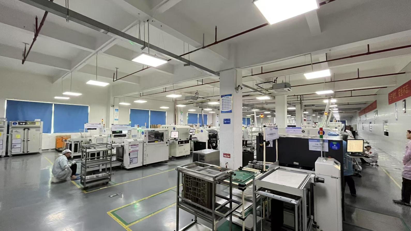
Modern Chinese exporters have migrated from labor-intensive assembly to fully automated Surface Mount Technology (SMT) and automated optical inspection (AOI) lines. Every RJ45 magnetic jack and SFP cage undergoes high-potential (Hi-Pot) dielectric testing, insertion loss measuring, and crosstalk analysis.
By pairing scalable volume production with zero-defect quality systems (ISO 9001:2015 compliant), global buyers gain access to tier-1 quality at a total cost of ownership (TCO) that cannot be matched by Western regional vendors.
Ensuring seamless international deployment through complete compliance with European, North American, and Asian telecom regulations.
100% compliance with EU Directives 2011/65/EU (RoHS 2.0) and REACH (EC 1907/2006). All lead-free soldering processes and non-hazardous plastic housings comply with stringent environmental guidelines.
Engineered to satisfy Class A and Class B EMI requirements. Integrated Faraday shielding cages prevent external radio frequency radiation from disrupting surrounding high-density server racks.
FiberNova offers worldwide technical field support, providing custom labeling, EEPROM vendor code programming (Cisco, Juniper, Arista coding), and specialized customs documentation for fast clearance.
How next-generation networking standards are driving hardware innovation in factories and export markets.
The global demand for high-speed network components is experiencing unprecedented expansion, driven primarily by generative AI workloads, hyperscale cloud data centers, and 5G/6G wireless infrastructure backhaul. As data transfer speeds shift rapidly from 10G and 100G toward 400G and 800G optical architecture, physical layer component manufacturers face new engineering challenges.
While optical transceivers are expanding into 400G/800G QSFP-DD and OSFP form factors, copper-based Ethernet interfaces remain essential for edge devices, industrial automation, and enterprise access switches. Modern factories are engineering hybrid RJ45 modular jacks capable of operating at 25GBASE-T and 40GBASE-T while maintaining strict backward compatibility with legacy 100BASE-TX and 1000BASE-T systems.
As smart buildings, Wi-Fi 6E/7 access points, and PTZ security cameras demand higher power levels directly over twisted-pair cables, network hub components must support up to 90W to 100W per port (PoE Type 4). Export-oriented factories must design transformers and magnetic jacks capable of handling continuous DC current up to 1A per pair without saturation or thermal degradation.
Global enterprise buyers increasingly demand optical transceivers pre-programmed with custom firmware to match proprietary host switch ecosystems. Exporters capable of offering real-time EEPROM recoding, DOM (Digital Optical Monitoring) calibration, and custom mechanical keying are capturing a dominant market share.
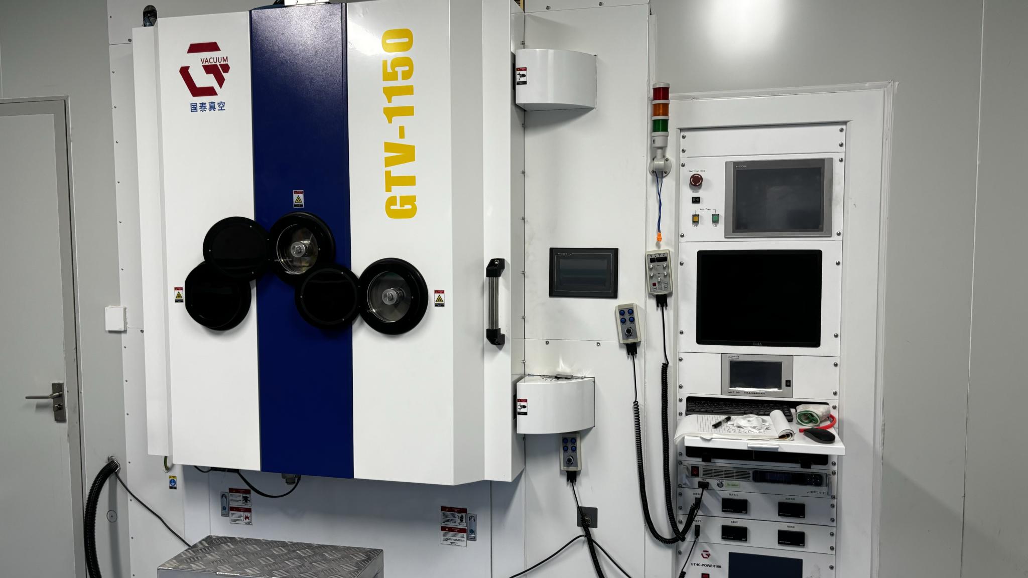
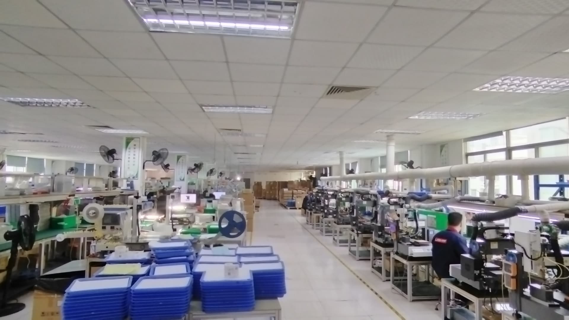
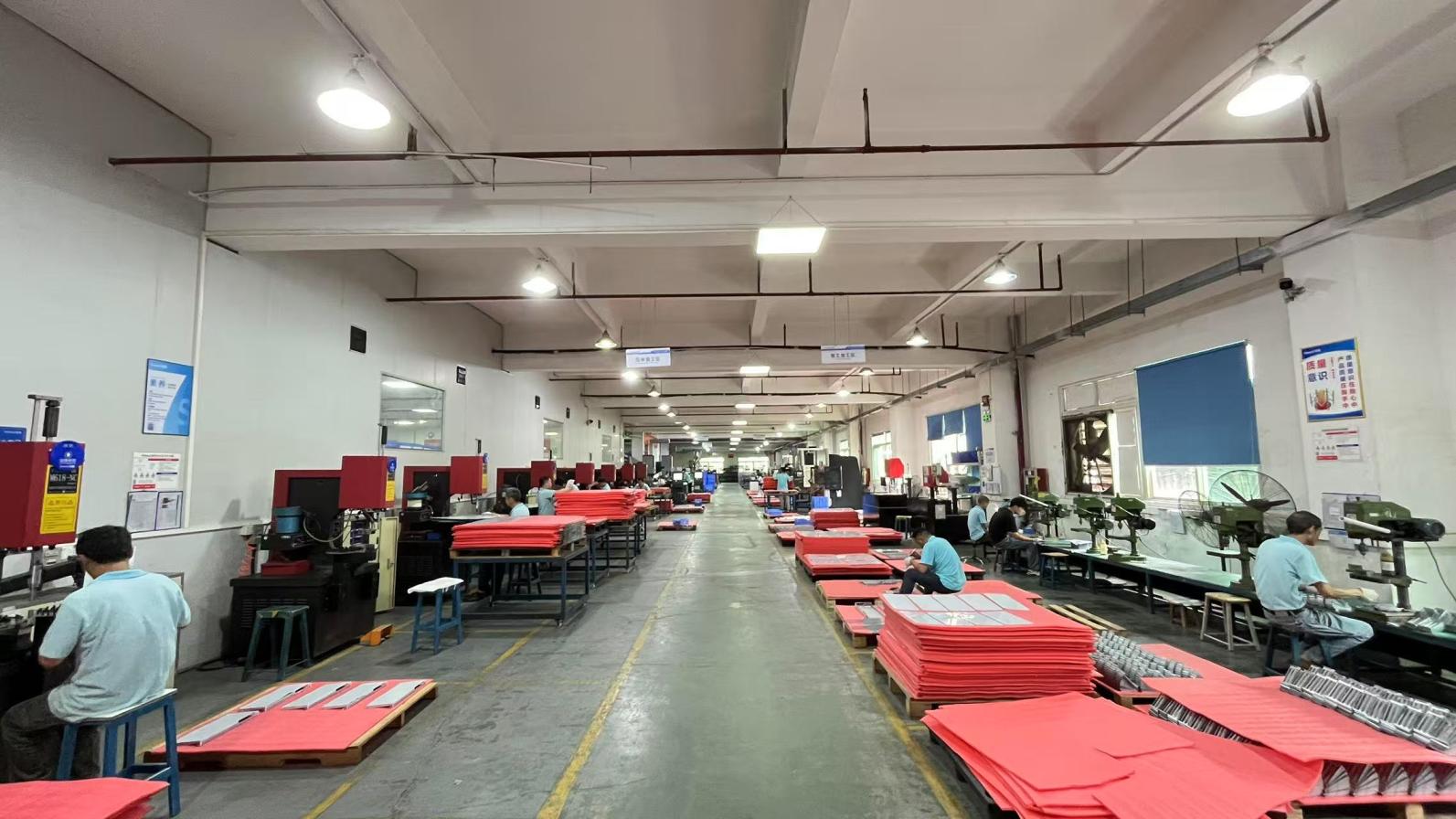
Visual evidence of cleanroom manufacturing, automated SMT lines, and optical spectrum testing equipment.
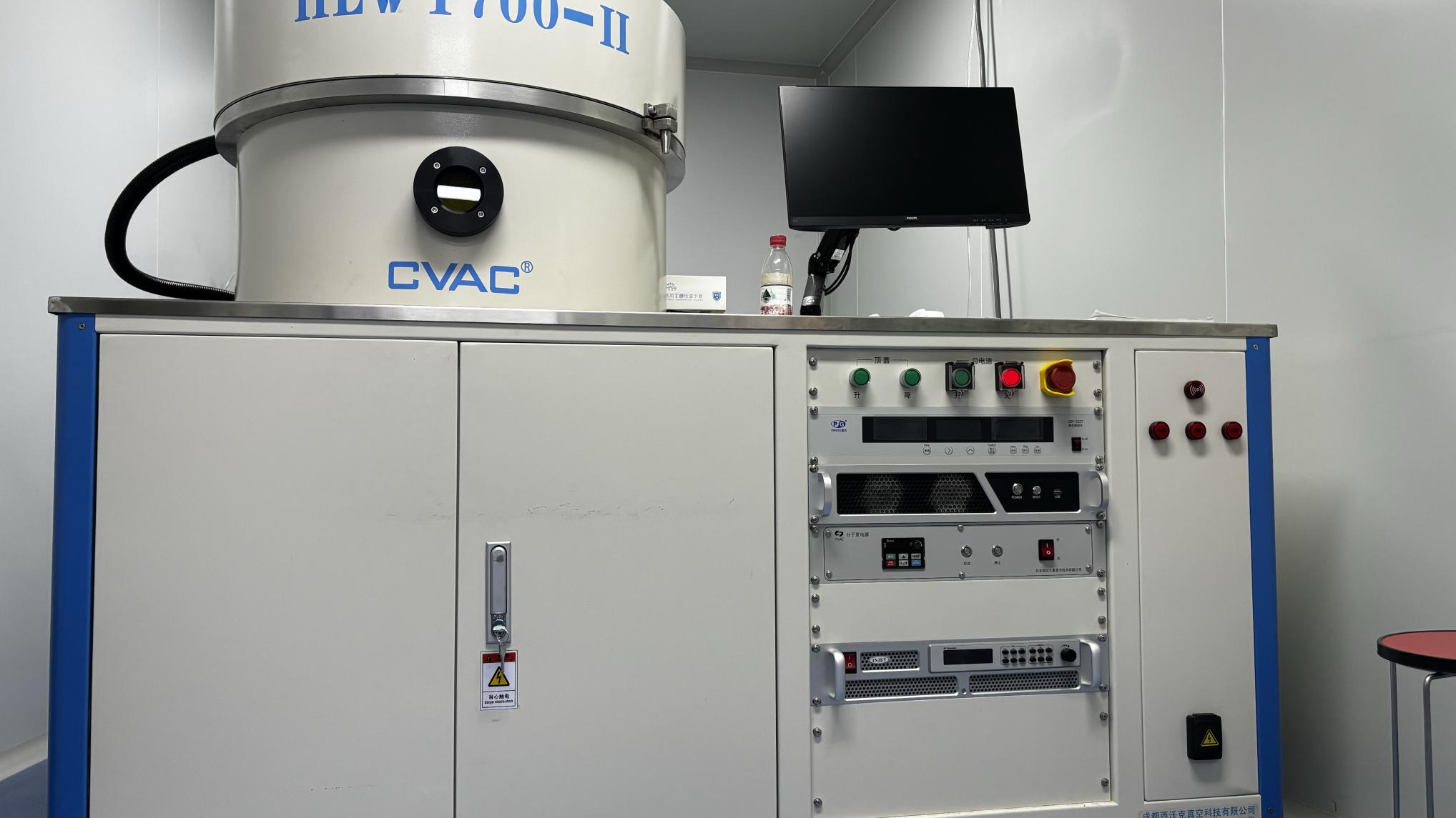
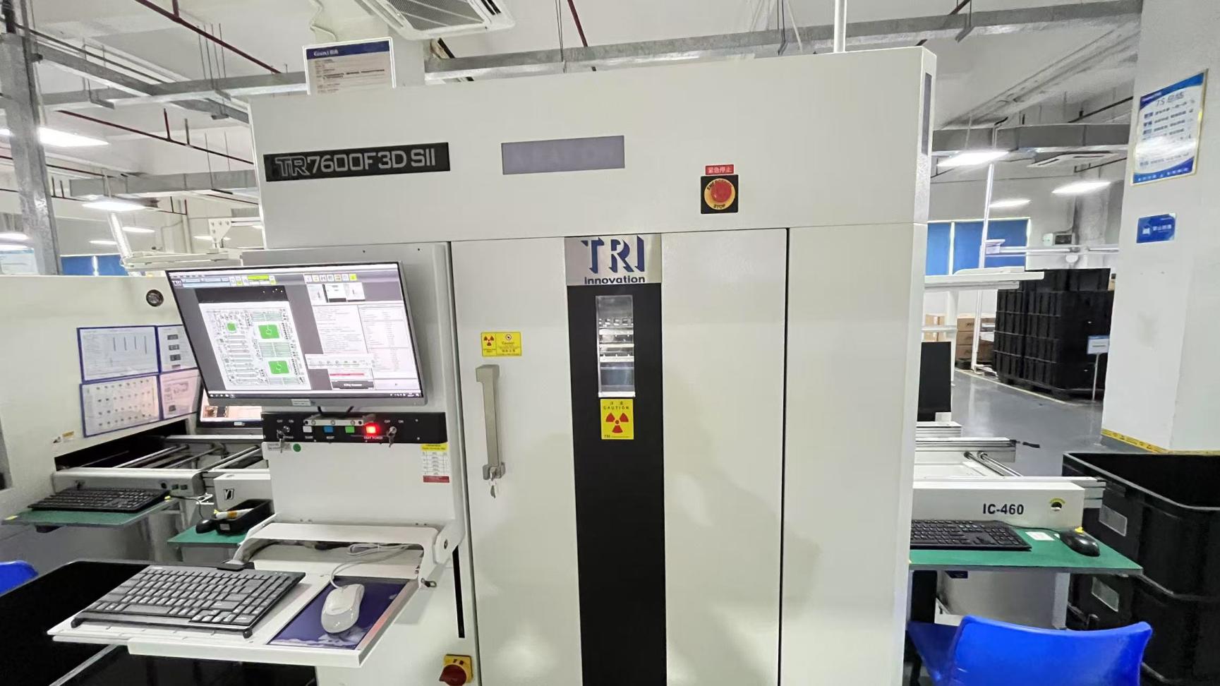
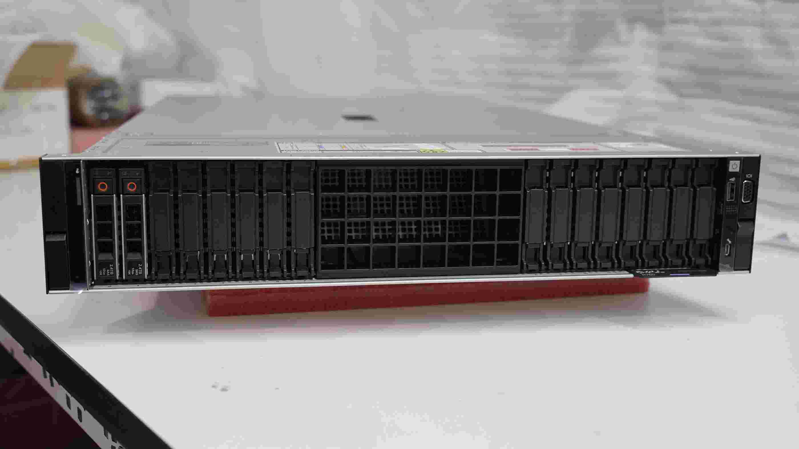

Industrial-grade components optimized for high-density switches, router backplanes, and telecom equipment.
Expert answers addressing common technical queries, compatibility concerns, and OEM logistics.
 FiberNova